
In today’s rapidly evolving electronics industry, precision and performance are essential. As devices become smaller and more complex, manufacturers are turning to advanced technologies to meet these demands. One such innovation is Hybrid Circuit Board Manufacturing, a process that combines multiple materials and technologies to create highly efficient and reliable electronic components. Understanding how this process works can provide valuable insight into the backbone of modern electronic systems.
What Is a Hybrid Circuit Board?
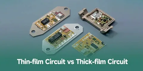
A hybrid circuit board is a specialized electronic assembly that integrates different types of substrates, components, and technologies into a single unit. Unlike traditional printed circuit boards (PCBs), hybrid boards can combine thick film, thin film, and surface-mount technologies. This allows for greater flexibility in design and improved electrical performance.
These boards are commonly used in industries where reliability is critical, such as aerospace, medical devices, telecommunications, and automotive systems. Their ability to handle complex functions in compact spaces makes them an ideal solution for high-performance applications.
Key Steps in the Manufacturing Process
The manufacturing of hybrid circuit boards involves several precise and carefully controlled steps. Each stage plays a vital role in ensuring the final product meets strict quality and performance standards.
1. Design and Material Selection
The process begins with detailed design planning. Engineers determine the layout, component placement, and electrical pathways based on the intended application. Material selection is equally important, as different substrates offer varying levels of conductivity, heat resistance, and durability.
Common materials include ceramics, glass, and specialized laminates. These materials are chosen to ensure optimal performance under specific operating conditions.
2. Substrate Preparation
Once the design is finalized, the substrate is prepared. This involves cleaning and conditioning the surface to ensure proper adhesion of conductive materials. A clean substrate is essential for achieving reliable electrical connections and preventing defects.
3. Deposition of Conductive Layers
In this stage, conductive materials are applied to the substrate to form electrical circuits. Techniques such as screen printing or vacuum deposition are used to create precise patterns. These conductive layers serve as the pathways for electrical signals.
The choice between thick film and thin film technologies depends on the application requirements. Thick film processes are generally more cost-effective, while thin film techniques offer higher precision and performance.
4. Component Placement and Attachment
After the circuit patterns are established, electronic components are placed onto the board. This can include resistors, capacitors, and integrated circuits. Advanced equipment ensures accurate placement, which is crucial for maintaining functionality and reliability.
Components are then securely attached using soldering or conductive adhesives. This step requires careful control to avoid damage and ensure strong connections.
5. Encapsulation and Protection
To protect the circuit from environmental factors such as moisture, dust, and temperature fluctuations, the assembly is encapsulated. Protective coatings or enclosures are applied to enhance durability and longevity.
This step is particularly important for applications in harsh environments, where exposure to extreme conditions could compromise performance.
6. Testing and Quality Assurance
The final stage involves rigorous testing to ensure the board meets all specifications. Electrical performance, durability, and reliability are evaluated through various tests. Any defects are identified and corrected before the product is approved for use.
Quality assurance is a critical part of the process, as it ensures that each board performs consistently and meets industry standards.
Advantages of Hybrid Circuit Boards
Hybrid circuit boards offer several benefits that make them a preferred choice for advanced applications:
● Compact Design: They allow for high-density component placement, reducing the overall size of devices.
● Enhanced Performance: Improved electrical characteristics result in better signal integrity and efficiency.
● Durability: The use of robust materials ensures long-term reliability.
● Customization: Designs can be tailored to meet specific application requirements.
These advantages make hybrid boards an essential component in modern technology.
Final Thoughts
As electronic devices continue to evolve, the demand for efficient and reliable circuit solutions grows. Hybrid Circuit Board Manufacturing represents a significant advancement in meeting these needs, combining precision engineering with innovative materials and processes. By understanding how these boards are created, it becomes clear why they are integral to high-performance applications across various industries. For those seeking expertise and quality in this field, At Hybrid-tek offers advanced solutions that reflect innovation, reliability, and technical excellence.

Write a comment ...